

Terahertz (THz) systems represent one of the next frontiers in electronics. THz applications are expected to include automotive advanced driver assistance systems (ADAS) for autonomous vehicles, next-generation telephony like 5G and 6G, augmented and virtual reality (AR & VR) technologies for the metaverse, and more. There will be numerous challenges to overcome in the development of THz electronics, and connectors and interconnection technologies will be one of the keys.
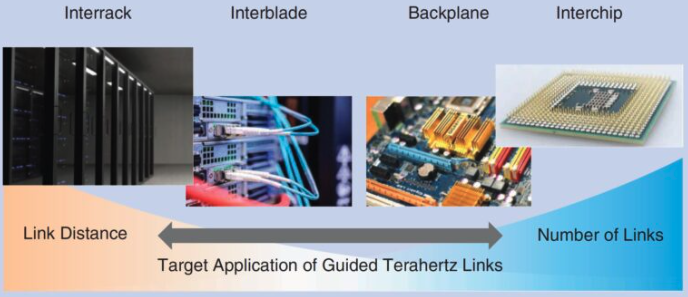
The THz band is often defined as frequencies from 0.1 to 3.0 THz, sitting between optical frequencies at the top end and microwave frequencies at the bottom. This FAQ will review the convergence of micro coaxial, waveguide, and fiber optic connections for THz systems and look at how those connectors will be used to bridge between different systems, within systems, and even within integrated circuits and system in package designs (Figure 1).
As frequencies continue to climb upward, using copper interconnects becomes more challenging. One way to increase data rates over copper is to limit the interconnect length. That’s not an uncommon strategy; Ethernet over copper data rates are doubling about every four years. At the same time, the maximum interconnect lengths for Ethernet over copper are being halved. That’s a necessary consequence of the inherent limitations of copper interconnects, but it raises a question about the efficacy of the doubling data rates.
As frequencies increase, the relative cost-performance gap between waveguides and copper shrinks. As frequencies approach the threshold that can justify using optical interconnects, waveguides can provide an option that is more robust to misalignment and cost-effective. At the upper end of the THz spectrum, a waveguide interconnect can have several orders of magnitude more tolerance to misalignment compared with optical interconnects and provide much lower losses compared to copper.
The boundaries between copper, waveguides, and optical interconnects are expected to continue shifting, with waveguides becoming more common. One key would be the commercial development of low-cost waveguide fabrication technologies similar to those currently used for twin axial cables. Of course, there is no perfect interconnect technology that can provide a panacea for all combinations of data rates, efficiencies, costs, and other requirements.
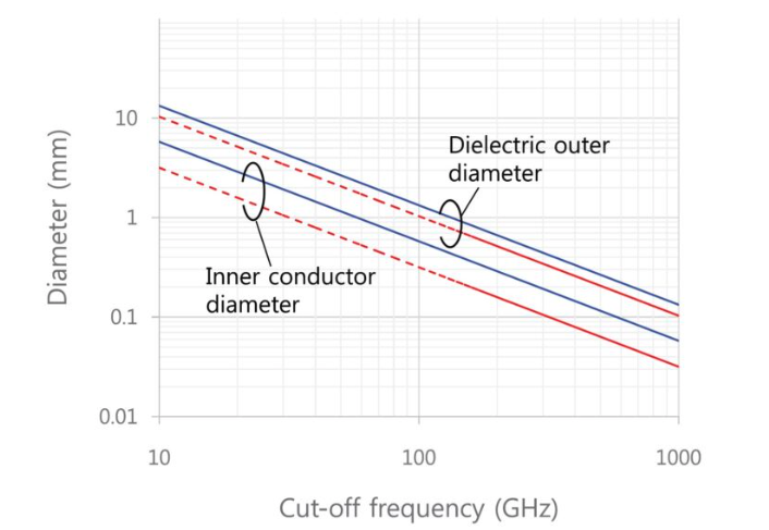
For example, conventional 50-Ω coaxial connectors may not be practical at THz frequencies even with modifications. Figure 3 illustrates the expected dimensions of 50-Ω coaxial connectors with respect to the cutoff frequency of the TE11 mode. TE11 mode is important since TE11 mode has the lowest cutoff frequency and is the dominant mode in a circular waveguide. Even with the dielectric between the inner and outer connectors eliminated, the center pin diameter is expected to be 0.2 mm for a 300 GHz cutoff frequency. Such a small center pin in a 50-Ω coaxial connector would not be reliable or durable in practical installations (Figure 3).
On the other hand, rectangular waveguides offer low losses in a highly durable, reliable, and repeatable mating system. Those waveguides may be the preferred connector geometry for THz systems, even though they are relatively bulky and typically have limited operating bandwidths. Waveguides can provide the best tradeoff between size and robustness at THz frequencies. For example, waveguide flange designs used in scientific and military systems have been optimized for repeatability and accuracy of mating. Applying those waveguide flange design concepts to commercial connectors could enable a new generation of THz connectors.
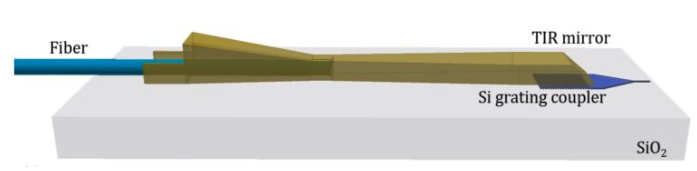
The funnel walls control light leakage by minimizing the fiber length, and the polymer waveguide is mode matched with the fiber. The light is coupled to a silicon waveguide using a total internal reflection (TIR) mirror and the grating coupler. The TIM mirror is fabricated at the same time as the funnel. The angled facet and the refractive index difference between the polymer and air are used by the TIR mirror to redirect the light into the grating coupler at the needed diffraction angle. The funnel is also a passive mechanical support and routing structure that optically aligns the fiber for edge coupling with the waveguide. By routing the fiber into the funnel independently of its exact position relative to the funnel’s center, wide alignment tolerances are supported (Figure 4).
In addition to the inherent grating coupler loss, the connector exhibited about 0.05 dB excess coupling loss between a high confinement silicon waveguide and a single-mode fiber waveguide. The resulting connector platform is expected to be scalable for various THz applications.
Testing demonstrated that the funnel connector design is robust for fiber mode field diameter (MFD) variations up to ±2 μm over a temperature range of 20 and 100 °C. Loss variations were within 0.6 dB over the entire temperature range. That compares very well with commercial photonic connectors, typically rated to a maximum of 70 °C. In addition, the dimensions and placement requirements of the proposed funnel connector are compatible with current high-volume microelectronic production tools. The platform fabrication can be done at the wafer level and does not require a cleanroom environment.
Reposted from the WeChat official account: qicheyanjiuyuanauto